- 您现在的位置:买卖IC网 > Sheet目录17351 > LM2595ADPBCKGEVB (ON Semiconductor)EVAL BOARD FOR LM2595ADPBCKG
�� �
�
�LM2595�
�PROCEDURE (ADJUSTABLE OUTPUT VERSION: LM2595)�
�Procedure�
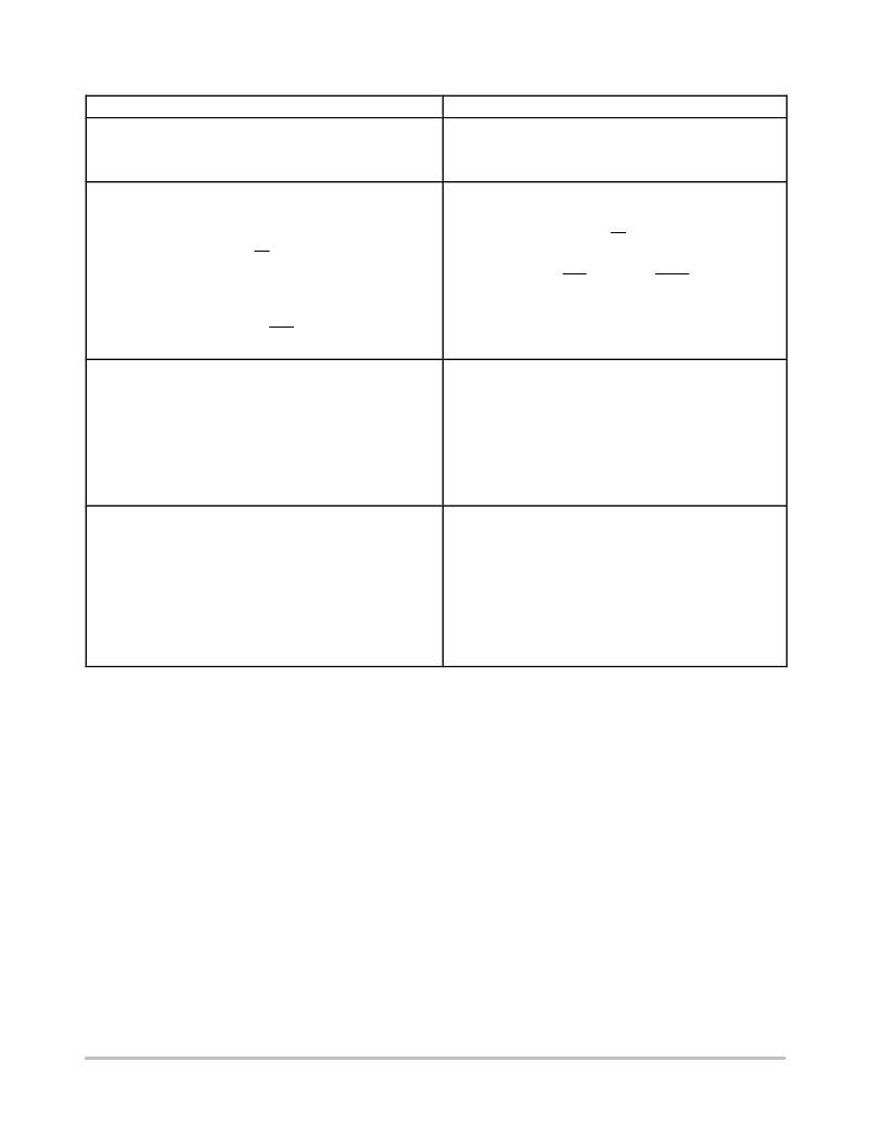
�Given� Parameters:�
�V� out� =� Regulated� Output� Voltage�
�V� in(max)� =� Maximum� DC� Input� Voltage�
�I� Load(max)� =� Maximum� Load� Current�
�1.� Programming� Output� Voltage�
�To� select� the� right� programming� resistor� R1� and� R2� value� (see�
�Example�
�Given� Parameters:�
�V� out� =� 5.0� V�
�V� in(max)� =� 12� V�
�I� Load(max)� =� 1.0� A�
�1.� Programming� Output� Voltage� (selecting� R1� and� R2)�
�Select� R1� and� R2:�
�1.0� )�
�V� out� +� V�
�where� V� ref� =� 1.23� V�
�V� out� +� 1.23� 1.0� )�
�V� out�
�R2� +� R1� *� 1.0�
�ref�
�+� *� 1.0�
�Figure� 1)� use� the� following� formula:�
�R2�
�ref� R1�
�Resistor� R1� can� be� between� 1.0� k� and� 5.0� k� W� .� (For� best�
�temperature� coefficient� and� stability� with� time,� use� 1%� metal�
�V�
�R2�
�R1�
�Select� R1� =� 1.0� k� W�
�5V�
�1.23� V�
�film� resistors).�
�R2� +� R1�
�V� out�
�V� ref�
�*� 1.0�
�R2� =� 3.07� k� W� ,� choose� a� 3.0k� metal� film� resistor.�
�2.� Input� Capacitor� Selection� (C� in� )�
�To� prevent� large� voltage� transients� from� appearing� at� the� input�
�and� for� stable� operation� of� the� converter,� an� aluminium� or�
�tantalum� electrolytic� bypass� capacitor� is� needed� between� the�
�input� pin� +V� in� and� ground� pin� GND� This� capacitor� should� be�
�located� close� to� the� IC� using� short� leads.� This� capacitor� should�
�have� a� low� ESR� (Equivalent� Series� Resistance)� value� .�
�For� additional� information� see� input� capacitor� section� in� the�
�“Application� Information”� section� of� this� data� sheet.�
�3.� Catch� Diode� Selection� (D1)�
�A.� Since� the� diode� maximum� peak� current� exceeds� the�
�regulator� maximum� load� current� the� catch� diode� current�
�rating� must� be� at� least� 1.2� times� greater� than� the� maximum�
�2.� Input� Capacitor� Selection� (C� in� )�
�A� 220� m� F,� 50� V� aluminium� electrolytic� capacitor� located� near�
�the� input� and� ground� pin� provides� sufficient� bypassing.�
�3.� Catch� Diode� Selection� (D1)�
�A.� For� this� example,� a� 1.0� A� (for� a� robust� design� 3.0� A� diode�
�is� recommended)� current� rating� is�
�adequate.�
�load� current.� For� a� robust� design,� the� diode� should� have� a�
�current� rating� equal� to� the� maximum� current� limit� of� the�
�LM2595� to� be� able� to� withstand� a� continuous� output� short.�
�B.� The� reverse� voltage� rating� of� the� diode� should� be� at� least�
�1.25� times� the� maximum� input� voltage.�
�B.� For� V� in� =� 12� V� use� a� 20� V� 1N5817� (1N5820)� Schottky�
�diode� or� any� suggested� fast� recovery� diode� in� the� Table� 2.�
�http://onsemi.com�
�9�
�发布紧急采购,3分钟左右您将得到回复。
相关PDF资料
R1S12-0505/P-R
CONV DC/DC 1W 05VIN 05VOUT
AS1329B EB
BOARD EVAL AS1329B
SJA7501-1-1/2-50-WHITE
LOOP WHITE 1 1/2" X 50YD 0.12"
ECM08DRYH
CONN EDGECARD 16POS DIP .156 SLD
CS51411EVB
EVAL BOARD FOR CS51411 HI FREQ
RBM06DCWD
CONN EDGECARD 12POS DIP .156 SLD
A9BAG-1604F
FLEX CABLE - AFF16G/AF16/AFE16T
TARQ224K035
CAP TANT 0.22UF 35V 10% AXIAL
相关代理商/技术参数
LM2595ATPBCKGEVB
功能描述:电源管理IC开发工具 LM2595ADJ TO220 BUCK DB
RoHS:否 制造商:Maxim Integrated 产品:Evaluation Kits 类型:Battery Management 工具用于评估:MAX17710GB 输入电压: 输出电压:1.8 V
LM2595DSADJG
功能描述:直流/直流开关调节器 1A BUCK SW REG 150KHZ RoHS:否 制造商:International Rectifier 最大输入电压:21 V 开关频率:1.5 MHz 输出电压:0.5 V to 0.86 V 输出电流:4 A 输出端数量: 最大工作温度: 安装风格:SMD/SMT 封装 / 箱体:PQFN 4 x 5
LM2595DSADJR4G
功能描述:直流/直流开关调节器 1A BUCK SW REG 150KHZ RoHS:否 制造商:International Rectifier 最大输入电压:21 V 开关频率:1.5 MHz 输出电压:0.5 V to 0.86 V 输出电流:4 A 输出端数量: 最大工作温度: 安装风格:SMD/SMT 封装 / 箱体:PQFN 4 x 5
LM2595S12
制造商:Texas Instruments 功能描述:SWITCHING REG, 1A 12V, SMD, 2595 制造商:Texas Instruments 功能描述:SWITCHING REG, 1A 12V, SMD, 2595; Primary Input Voltage:24V; No. of Outputs:1; Output Voltage:12V; Output Current:1A; Voltage Regulator Case Style:TO-263; No. of Pins:5; Operating Temperature Min:-25C; Operating Temperature ;RoHS Compliant: Yes
LM2595S-12
功能描述:直流/直流开关转换器 RoHS:否 制造商:STMicroelectronics 最大输入电压:4.5 V 开关频率:1.5 MHz 输出电压:4.6 V 输出电流:250 mA 输出端数量:2 最大工作温度:+ 85 C 安装风格:SMD/SMT
LM2595S12
制造商:Texas Instruments 功能描述:IC SWITCHING REG 1A 12V SMD 2595
LM2595S-12/NOPB
功能描述:直流/直流开关转换器 RoHS:否 制造商:STMicroelectronics 最大输入电压:4.5 V 开关频率:1.5 MHz 输出电压:4.6 V 输出电流:250 mA 输出端数量:2 最大工作温度:+ 85 C 安装风格:SMD/SMT
LM2595S-3.3
功能描述:直流/直流开关转换器 RoHS:否 制造商:STMicroelectronics 最大输入电压:4.5 V 开关频率:1.5 MHz 输出电压:4.6 V 输出电流:250 mA 输出端数量:2 最大工作温度:+ 85 C 安装风格:SMD/SMT